
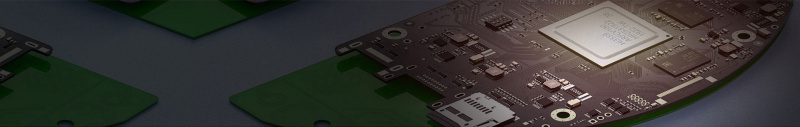
What is a four-layer pcb?
- Author:Admin
- Time:2023-06-08
- Browse:
What is a four-layer pcb?
Due to the development of electronic products towards high precision, traditional double-sided boards can no longer meet the needs of most products, and design engineers increasingly favor four-layer boards. So what is the difference between four-layer boards and double-sided boards?
The four-layer board is based on the double-sided board and then pressed. When pressed, PP and copper foil are added to both sides of the double-sided board, and then pressed into a multi-layer board under high temperature and pressure. Simply put, a four-layer board has an inner layer. In terms of process, some circuits are etched through the inner layer and then pressed and formed. Double panel refers to the process of directly cutting the incoming sheet material and then drilling and making it.
Although it is difficult to obtain a four-layer board by looking at the cut surface of the PCB board, few people have this kind of insight. But by observing the guide holes, the four-layer board can be identified. If the same guide holes can be found on both sides of the PCB board, or if the motherboard or display card is facing the light source, and if the position of the guide holes is not transparent, it is a four-layer board.
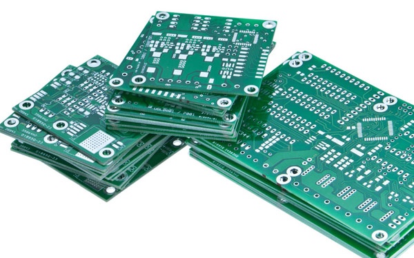
Do you know which four-layer PCB board is?
The four layers in the four-layer PCB board are divided into: the signal layer (top layer), signal layer (bottom layer), power layer (middle layer), and ground layer (middle layer).
Usually in a circuit board, the top layer is usually placed with components, so the top layer is also called the component surface; The bottom layer is usually used for welding, so the bottom layer is also called the welding surface. But for SMD components, both the top and bottom layers can accommodate components.
The layout of each layer of the four-layer PCB board:
1. The first layer in the middle has multiple GNDs laid separately, and a small number of wires can be used, but do not divide each layer of copper; The second layer of VCC copper laying in the middle has multiple power supplies laid separately, and a small number of wires can be used, but do not divide each layer.
2.There are four wiring layers, usually the top layer of TOP LAYER, the bottom layer of Button Layer, and the four layers of VCC and GND. Generally, through-holes, buried holes, and blind holes are used to connect each other's layers, which adds an additional buried hole and blind hole compared to double-layer PCB boards. In addition, VCC and GND layers should avoid using signal cables as much as possible.
Disclaimer: All works (images, text, audio, and video) on this website are compiled from internet sources for the purpose of learning and communication among users. If your rights have been infringed, please contact the administrator to request removal.
URL:http://www.worthpcb.com/index.php?c=article&id=194
Recommend Article
- What is a four-layer pcb?
- What is double-layer PCB?
- We often encounter special process problems d...
- When you start to assemble, you must need a s...
- Professional Surface-mounting and Through-hol...
- Multilayer PCB provide higher design flexibil...
- HDI PCB is typically made using the following...
- What is HDI PCB?
- Why is FR4 prioritized as the PCB base materi...
- Professional Custom PCB and PCBA manufacturer...
- High-Quality PCB Manufacturer Multi-layer PCB
- Customized FR4 Double Layer PCB