
What is double-layer PCB?
- Author:Admin
- Time:2023-06-08
- Browse:
What is double-layer PCB?
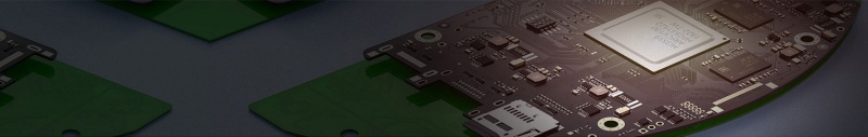
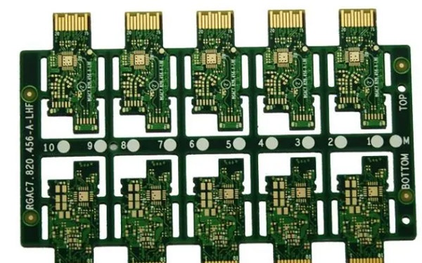
The double-sided board is the printed circuit board with copper on both sides including the Top (top layer) and the Bottom (bottom layer). It is the most common and versatile circuit board. The connection is mainly through vias or pads. Because both sides can be wired, which greatly reduces the difficulty of wiring, it is widely used.
There are wirings on both sides of the double-sided board, but to use the wires on both sides, there must be an appropriate circuit connection between the two sides. The "bridge" between the circuits is called a guide hole. The guide hole is a small hole filled or coated with metal on the PCB, which can be connected to the wires on both sides. Because the area of the double-sided panel is twice as large as that of the single-sided panel, the double-sided panel solves the difficulty of interlacing wiring in the single-sided panel (it can be conducted to the other side through holes), and it is more suitable for circuits that are more complex than the single-sided panel.
The production of double-sided panels is more complicated than that of single-sided panels. The main reasons are as follows:
(1) The top and bottom layers of the copper-clad board must be wired.
(2) The wires on the top and bottom layers should be connected with metalized vias.
Among them, metallization is particularly critical, which is also the core process of double-sided panel production. The so-called via metallization is to coat a layer of metal on the inner wall of the via a hole in order to connect the printed wires of the top layer and the bottom layer. At present, domestic via-hole metallization mainly adopts the electroless copper plating process. There are two types of electroless copper plating processes:
① Thin copper is electroless plated first, then the whole board is electroplated to thicken the copper layer, and then the pattern is transferred.
② Thick copper plating by electroless first, and then transfer graphics directly.
Both are widely used. However, the electroless copper plating method is harmful to the environment, and it will gradually be replaced by more advanced black hole technology, tin/palladium direct plating technology, and polymer direct plating technology.
Disclaimer: All works (images, text, audio, and video) on this website are compiled from internet sources for the purpose of learning and communication among users. If your rights have been infringed, please contact the administrator to request removal.
URL:http://www.worthpcb.com/index.php?c=article&id=193
Recommend Article
- What is a four-layer pcb?
- What is double-layer PCB?
- We often encounter special process problems d...
- When you start to assemble, you must need a s...
- Professional Surface-mounting and Through-hol...
- Multilayer PCB provide higher design flexibil...
- HDI PCB is typically made using the following...
- What is HDI PCB?
- Why is FR4 prioritized as the PCB base materi...
- Professional Custom PCB and PCBA manufacturer...
- High-Quality PCB Manufacturer Multi-layer PCB
- Customized FR4 Double Layer PCB