
Multilayer PCB provide higher design flexibility and complexity by combining multiple layers.
- Author:Admin
- Time:2023-06-08
- Browse:
Multilayer PCB provide higher design flexibility and complexity by combining multiple layers.
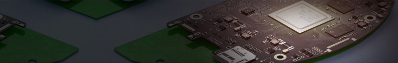
Multilayer PCB (Printed Circuit Board) refers to a type of PCB that consists of multiple layers of conductive traces and insulating material stacked together. Unlike single-layer or double-layer PCB, which have only one or two layers of conductive material, multilayer PCB provides increased design flexibility and complexity by incorporating multiple layers.
In a multilayer PCB, the layers are interconnected using vias, which are small plated holes that allow electrical connections between the different layers. These vias can be through-hole vias, which traverse through all the layers, or they can be blind vias, which connect one or more inner layers but do not traverse the entire board, or buried vias, which connect inner layers without being exposed on the outer layers.
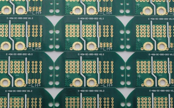
The construction of a multilayer PCB typically includes the following layers:
Signal Layers: These layers contain the conductive traces that carry electrical signals and provide interconnections between components on the PCB.
Power and Ground Plane Layers: These layers are dedicated to providing power supply and ground connections. They help distribute power and minimize electromagnetic interference.
Insulating Layers (Prepreg): Insulating layers, also known as prepreg layers, consist of a dielectric material such as fiberglass or epoxy resin. They separate the conductive layers to prevent short circuits and provide structural integrity.
The number of layers in a multilayer PCB can vary depending on the complexity of the circuit design and the specific requirements of the application. Commonly used multilayer PCB configurations include 4-layer, 6-layer, 8-layer, and even higher layer counts.
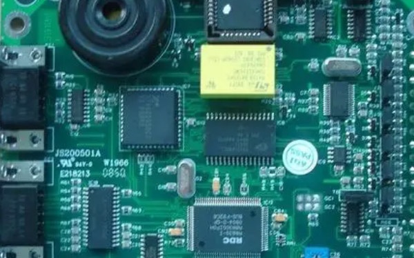
Multilayer PCB offers several advantages over single-layer or double-layer PCB. They allow for higher circuit density, reduced board size, improved signal integrity, and enhanced electromagnetic compatibility (EMC). Additionally, multilayer PCB are suitable for complex electronic systems that require a high degree of integration and functionality.
The manufacturing of multilayer PCB involves advanced processes such as layer alignment, lamination, drilling, and copper plating. These processes require specialized equipment and expertise to ensure precise layer registration and reliable interconnections between layers.
Multilayer PCB is widely used in various industries, including telecommunications, computing, automotive, medical devices, aerospace, and industrial equipment, where space optimization and high-performance circuitry are crucial.
Disclaimer: All works (images, text, audio, and video) on this website are compiled from internet sources for the purpose of learning and communication among users. If your rights have been infringed, please contact the administrator to request removal.
URL:http://www.worthpcb.com/index.php?c=article&id=189
Recommend Article
- What is a four-layer pcb?
- What is double-layer PCB?
- We often encounter special process problems d...
- When you start to assemble, you must need a s...
- Professional Surface-mounting and Through-hol...
- Multilayer PCB provide higher design flexibil...
- HDI PCB is typically made using the following...
- What is HDI PCB?
- Why is FR4 prioritized as the PCB base materi...
- Professional Custom PCB and PCBA manufacturer...
- High-Quality PCB Manufacturer Multi-layer PCB
- Customized FR4 Double Layer PCB