
What is HDI PCB?
- Author:Admin
- Time:2023-06-08
- Browse:
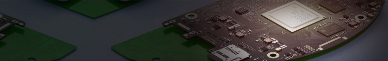
HDI PCB stands for High-Density Interconnect Printed Circuit Board. It is a specialized type of printed circuit board designed to achieve higher component density and more complex interconnection structures in smaller form factors.
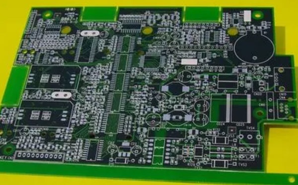
HDI PCB employs advanced technologies and manufacturing processes to minimize the size of the circuit board and provide higher routing density. They typically utilize multilayer construction with micro-sized traces, fine pitch, and the use of blind vias and buried vias to achieve highly integrated circuit layouts.
HDI PCB offers several advantages. Firstly, they allow for more electronic components to be accommodated in a smaller space, providing higher functional density. Secondly, HDI PCB provides shorter signal paths, lower resistance, and inductance, improving signal integrity and performance. Additionally, HDI PCB exhibits better resistance to interference and higher reliability.
HDI PCB finds extensive applications in mobile communication devices, computers, consumer electronics, medical equipment, automotive electronics, and other fields that demand miniaturization, lightweight design, and high performance.
In summary, HDI PCB is an advanced printed circuit board used for achieving high-density routing and complex interconnections. By employing advanced technologies and manufacturing processes, they meet the requirements of modern electronic devices for compact size, high performance, and reliability.
Disclaimer: All works (images, text, audio, and video) on this website are compiled from internet sources for the purpose of learning and communication among users. If your rights have been infringed, please contact the administrator to request removal.
URL:http://www.worthpcb.com/index.php?c=article&id=187
Recommend Article
- What is a four-layer pcb?
- What is double-layer PCB?
- We often encounter special process problems d...
- When you start to assemble, you must need a s...
- Professional Surface-mounting and Through-hol...
- Multilayer PCB provide higher design flexibil...
- HDI PCB is typically made using the following...
- What is HDI PCB?
- Why is FR4 prioritized as the PCB base materi...
- Professional Custom PCB and PCBA manufacturer...
- High-Quality PCB Manufacturer Multi-layer PCB
- Customized FR4 Double Layer PCB