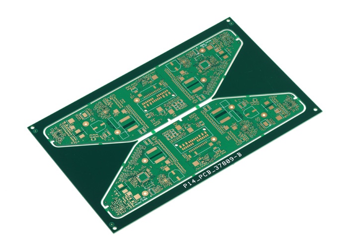
Multilayer PCB
- Author:Admin
- Time:2023-06-05
- Browse:
Product Introduction
| Place of Origin: | Shenzhen, China |
| Material Brand: | KB |
| Base Material: | FR4 TG140 |
| Layer: | 2 layers |
| Board size: | 36.2*69.2mm/2pcs |
| Copper Thickness: | 1oz |
| Board Thickness: | 1.6mm |
| Min. Hole Size: | 0.15mm |
| Min. Line Width: | 3 Mil |
| Min. Drilling: | 0.1mm |
| Surface Finishing: | ENIG |
Color
Black solder mask and White silkscreen
Supply Ability
50000 sqm/month
Packaging & Shipping
Packaging Details: Vacuum packagingWe can ship by DHL/FedEx/EMS/CHINA POST OFFICE and so on.
Generally speaking, the detailed shipping days are as below.
1 DHL: 3-7 DAYS
2 FedEx: 4-8 DAYS
3 EMS: 5-10 DAYS
4 CHINA POST OFFICE: 20-25 DAYS
Our Services
1. Quick response2. Reasonable price based on good quality
3. Provide one-stop service(components, OEM)
4. Abundant inventory & Habitual material preparation
FAQ (PURCHASING TIPS)
1. What file formats do you accept for production?A: Gerber file
2. Are my files safe?
A: Your files are held in complete safety and security. We protect the intellectual property of our customers throughout the whole process. All documents from customers are never shared with any third parties.
3. Shipping cost?
A: The shipping cost is determined by the destination, weight, and packing size of the goods. Please let us know if you need us to quote you the shipping cost.
Disclaimer: All works (images, text, audio, and video) on this website are compiled from internet sources for the purpose of learning and communication among users. If your rights have been infringed, please contact the administrator to request removal.
URL:http://www.worthpcb.com/index.php?c=article&id=166