PCB Manufacturing is the construction of your board design. This is a two-step process that begins with board fabrication and ends with printed circuit board assembly (PCBA). Mainly Double-sided PCB, 4-Layers PCB, Multilayers PCB, and PCBA. That's what we do.
Double-Sided PCB
Double-sided PCB have a conductive layer on each side. A dielectric layer is surrounded by circuit copper layers and solder mask on both sides. There is an abundance of applications and electronics in which double-sided PCB can be used in electronics such as LED lighting systems, Amplifiers, Car dashboards, Industrial controls, etc.
4-layer PCB
4-layer PCB are PCB that have four conductive layers: the top layer, two inner layers, and the bottom layer. Both inner layers are the core, usually used as power or ground planes, while the top and bottom outer layers are for placing components and routing signals.
Multilayer PCB
Multilayer PCB can support a high level of circuit complexity as they are made up of three or more copper layers laminated together. Multilayer PCB are more durable and tough after the curing process. They can be used in electronic devices such as Fiber optics, Smartphones, GPS systems, etc.
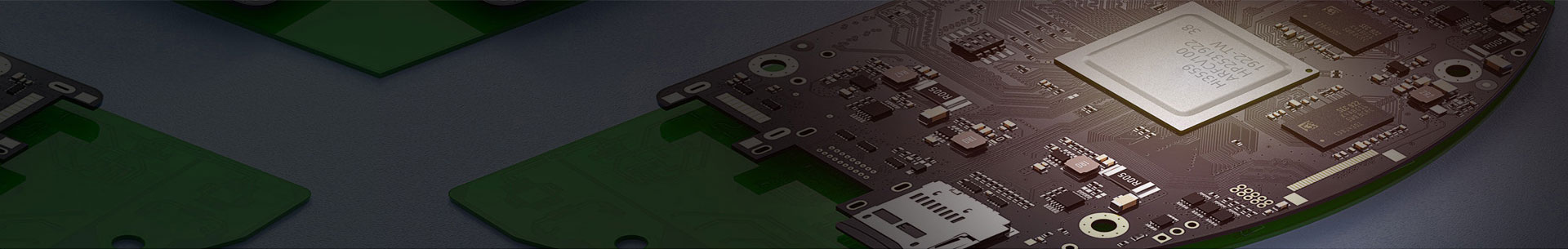
PCBA
Once a PCB is ready, it has to be assembled with active and passive electronic components. Once all the electronic components are assembled or soldered onto the PCB it is termed a PCBA or Printed Circuit Board Assembly. Now the board is ready to be used in the electronic device that it was designed for.